ABSTRACT
In order to accurately reconstruct signal waveform a signal must be sampled at least twice as fast as the bandwidth of the signal. Ultra Wideband (UWB) signals have extraordinary potential for high information transmission while a central focus of wireless has been the mobile communication. It is an emerging area that involves development of RF sensing and spectral applications over multiple GHz bandwidths. Even though our technology is improving, it is very challenging to build ADC’s that are compatible and keep up with the growth of ultra-wide band range.
Compressive sensing does “sampling” and “compressing” at the same time and exploits the sparsity for commensurate power saving by enabling sub-Nyquist under-sampling acquisition. The main idea behind compressive sensing is to recover specific signals from very few samples as compared to conventional Nyquist samples. In this thesis, a compressive sensing front-end (CSFE) is designed and analyzed to mitigate sampling approach limitations of the architecture in a CMOS process.
CSFE has four main components: pseudo random sequence generator (PBRS), multiplier, integrator, and ADC. The PBRS (implemented by a Gold code generator) and the multiplier are designed in Cadence Spectre using TSMC 180nm technology. The integrator and the 10-bit ADC are designed and verified using both Verilog-A and Matlab. Using 4 GHz PBRS and 800 MHz under sampling ADC, the CSFE design can detect signal frequency up to 2 GHz after applying the Orthogonal Matching Pursuit algorithm to reconstruct the under-sampling ADC data.
COMPRESSION SENSING
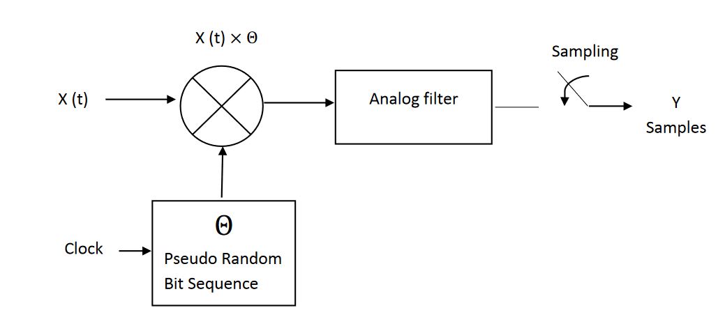
Fig . 2.4 Architecture of AIC
Advances in Digital Signal Processing (DSP) has numerous applications in the field of wireless communication, multimedia, biomedical and in radar detection systems. Digital Signal Processing converts any signal to digital domain for the processing part and we do this analog to digital conversion to get rid of complex design consideration of analog handling like noise figure, feed through and linearity and that is where the analog to digital converter(ADC) comes in to picture.
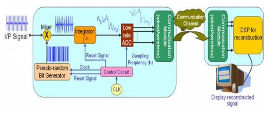
Fig . 2.5 Hardware block diagram of RD
In 2007, a research team from the rice university presented the first analog front end design for the compressed sensing and named it Random Demodulator (RD). RD uses Pseudo Random Bit Sequence (PBRS) to generate random sequence which can be used as a measurement matrix and after that it multiplies input signal which must be sparse or compressible with the random sequence generated by PBRS. RD uses Maximal-Length Linear Feedback Shift Register (MLFSR) as a PBRS, it generates sequence of 2n–1 bits for n number of shift registers.
RANDOM DEMODULATOR IN TSMC 18 0NM CMOS TECHNOLOGY
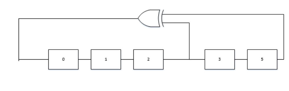
Figure 3.2 LFSR using Fibonacci Implementation
The Fibonacci implementation is most commonly used type of LFSR, It is also known as Simple type or out of line LFSR. In this implementation data flowing is done from left to right and feedback path is reverse of that, right to left. The bit positions that have an impact on next input bit are called taps. The furthest right bit is called output bit and polynomial order of the shift register increments from right to left. Figure 3.2 displays the block diagram of the Fibonacci implementation.
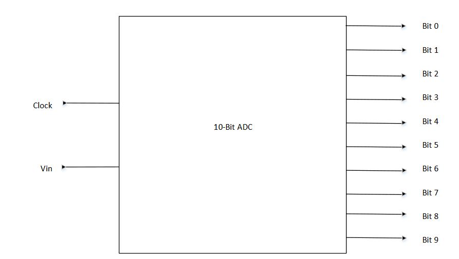
Figure 3.2 1 Symbol of ADC
The output of integrator is fed to the low sampling ADC where the integrated signal is sampled at a low sampling frequency as compared to the Nyquist frequency. Our aim for this ADC is to verify the compressive sensing front-end design. We create a software model of 10-bit ADC in system Verilog (Verilog-A), which is included in Appendix. We can change parameters of ADC by just changing the variables in the code. Figure 3.21 shows the symbol of the ADC. Figure 3.22 shows waveform of the ADC, in which the input signal dynamic range is from -0.25 V to 0.25 V and the 10-bit ADC output sample value is from 0 to 1023.
COMPRESSIVE SENSING FRONT-END (CSFE) PERFORMANCE EVALUATION
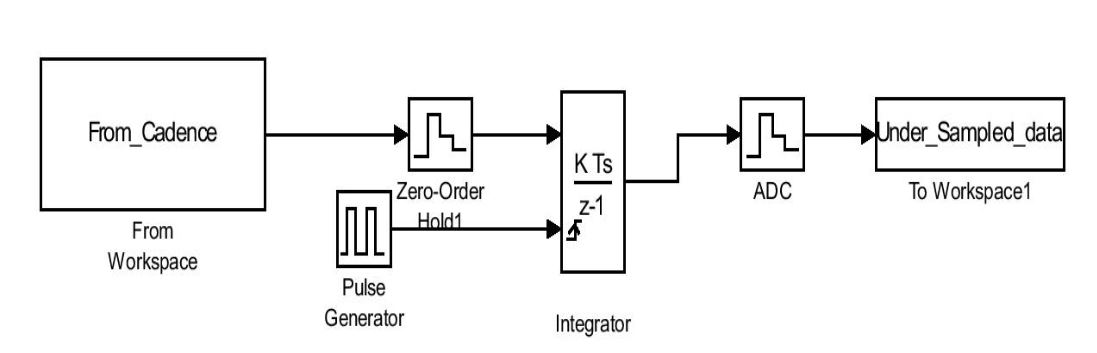
4.3 CSFE using Cadence and Simulink blocks
Figure 4.3 displays the final design of CSFE where the first block is the output of the cadence design. Other blocks are integrator and ADC in Simulink. The output of figure 4.3 is under sample data for signal reconstruction using Orthogonal Matching Pursuit (OMP). The measurement matrix Φ is built according to the G old code. One example of how to construct measurement matrix is given below.
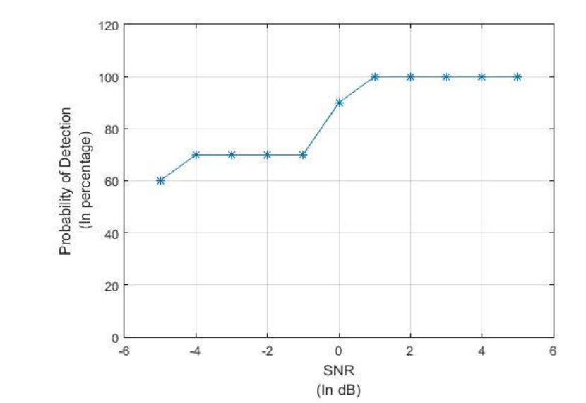
Figure 4.4 Sensitivity curve for 4 GHz
The proposed CSFE design and OMP successfully function at 4 GHz sampling rate. The sensitivity curve at 4GHz is shown in figure 4.4. The X-axes is SNR of input signal and Y-axes is probability of signal detection after OMP. For very case of SNR (from -5 to +5 dB) we randomly generate 10 signal frequency cases. The probability of signal detection is 100% at SNR from +1 to +5 dB, 90% at SNR of 0 dB, 70% at SNR from -1 to -4 dB, and 60% at SNR of -4 dB. The receiver sensitivity is 0 dB.
CONCLUSION AND FUTURE WORK
In this research, we have investigated the new field of compressed sensing and proposed a front-end design for CS. We have proposed architecture design of CSFE, component designs using Cadence virtuoso in CMOS 180nm technology and Cadence using Verilog-A. We also built a CSFE design in Simulink to verify the performance of the proposed design. We have proposed Gold code generator in cadence, which can run up to 5 GHz.
The Gold code generator is used as a pseudo random sequence generator. The length of the gold code sequence is also an important factor in the compressed sensing. The proposed design did not work for the 31 bits repetitive sequence but it worked perfectly fine for the 127 bits of repetitive sequence. A CMOS transistor design of multiplier has been presented in cadence. Ideal designs of integrator and ADC are presented in both Cadence Verilog-A and Simulink.
We use OMP algorithm to reconstruct the under sample data. The new proposed design is able to reconstruct Nyquist data at 5 times under sampling rate of the Nyquist rate. The proposed design operates at 4 GHz and the ADC operates at an under sampling frequency of 800MHz, five times lower than the Nyquist rate. We have also evaluated the performance of CSFE and OMP for different input signal SNR. The receiver sensitivity is 0 dB.
Source: Wright State University
Author: Julin Mukeshkumar Shah
>> 50+ Matlab projects for Digital Image Processing for Engineering Students
>> More Matlab Projects on Signals and Systems for Engineering Students
>> More Analog Communication Projects using Matlab for Final Year Students
>> More Matlab Engineering Projects based on Wireless Communication for Students
>> More Wireless Communication Projects in Matlab for Final Year Students