ABSTRACT
In analog signal processing the squaring circuit represents the core for implementing an analog signal having a value representing the square of the input signal. For example, calculating the square of input signal is necessary in adaptive processing of an input signal based on its instantaneous root mean square value.
In this thesis, a new 1-Ghz analog signal squaring circuit (squarer) designed in 180 nano meter CMOS process is presented. It is implemented by CMOS components including current source, current mirror, differential amplifier, low-pass filter, and voltage output buffer. A gain control amplifier and a 10-bit ADC are set up to evaluate the dynamic performance of the CMOS signal squarer. The measured results show a wide sweep capability of analog signal frequency up to 1 GHz with good linearity and spurious-free dynamic range.
CMOS SIGNAL SQUARING CIRCUIT
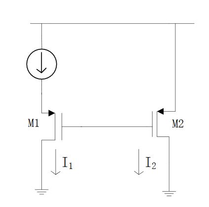
Figure 2.3 NMOS Current mirror
A current mirror is defined as a circuit designed to copy a current through one active device by controlling the current in another active device of a circuit, keeping the output current constant regardless of loading. Conceptually, an ideal current mirror is an ideal inverting current amplifier. Current mirror has three main parameters. 1) the transfer rate (transfer radio), also called the current amplification factor, 2) the AC output resistance, determined by the output current and voltage, and 3) the lowest working voltage, i.e., the minimum voltage to make the current mirror work.
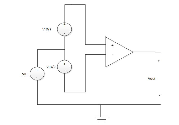
Figure 2.5 Differential Amp
For differential signal mode, the input signal equal to the difference of v1 and v2. vID represents the input signal as shown in Fig. 2.5. In this case, differential amp amplified the difference between two input signals.
1-GHZ CMOS SIGNAL FREQUENCY SQUARER
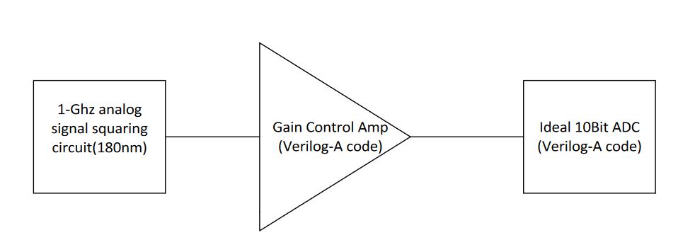
Figure 3.6 Test bed to evaluate the signal squarer
In order to evaluate dynamic performance of the signal squarer, a test bed is set up in Fig. 3.6. The square output of the frequency squarer is fed to a gain control amp, which adjust the square output dynamic range and the DC offset voltage to meet the 10-bit ADC specifications.
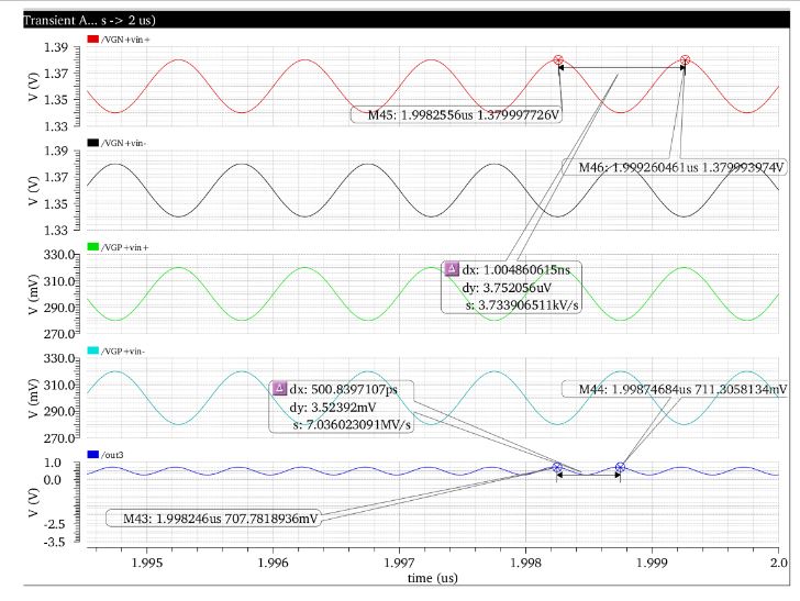
Figure 3.15 The differential amplifier four input signals
Applying 1 Ghz input signal, the differential amplifier input and the square output wave forms are shown in Fig. 3.15 where the yellow, green, light blue and blue wave forms are the four input signals.
CONCLUSION
Conclusion
In this research, the proposed analog signal squaring circuit maintains good linearity and achieves high SFDR for input signal frequency up to 1-Ghz. Three design challenges were observed. They are:
(1) The roll of current source and current mirror is important, which provides a stable DC bias voltage at an analog input signal to ensure that the next stage difference amplifier can function properly to square the input signal. If the DC bias voltage of the input signal is not in the correct range, the signal squaring function can not be achieved.
Future Work
My future research includes:
(1) Increase input signal frequency range from 1 Ghz to 2~3 Ghz. Improve my current differential amplifier design to function in a wider bandwidth while keep linearity and high SFDR for the squared output waveform.
(2) Design new current sink source and current mirror circuit to provide DC bias voltage to the wide bandwidth differential amplifier and reduce the input noise.
(3) Design a new noise reduction filter in a wider bandwidth for the signal squaring output to improve the linearity and SFDR.
Source: Wright State University
Author: Lizhong He