ABSTRACT
The paper presents a fully-integrated and universal DC/DC converter to minimize cost and size of power supply systems in wireless nodes for Internet-of-Things (IoT) applications. The proposed converter avoids the use of inductors and is made by a cascade of switching capacitor stages, implementing both step-down and step-up converting ratios, which regulate input sources from 1V to 60V to a voltage of about 4V. Multiple linear regulators are placed at the end of the cascade to provide multiple and stable output voltages for loads such as memories, sensors, processors, wireless transceivers. The multi-output power converter has been integrated in a Bipolar-CMOS-DMOS (BCD) 180nm technology.
As case study, the generation of 3 output voltages has been considered (3V, 2.7V, and 1.65V with load current requirements of 0.3A, 0.3A, and 0.12A, respectively). Thanks to the adoption of a high switching frequency, up to 5MHz, the only needed passive components are flying capacitors, whose size is below 10nF, and buffer capacitors, whose size is below 100nF. These capacitors can be integrated on top of the chip die, creating a 3D structure. This way, the size of the power management unit for IoT and CPS nodes is limited at 18mm2. The proposed converter can also be used with changing input power sources, like power harvesting systems and/or very disturbed power supplies.
MODELS AND ARCHITECTURE OF THE MULTI-OUTPUT SWITCHED CAPACITOR CONVERTER
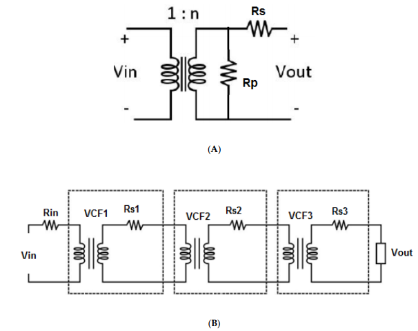
Figure 1. (A) Equivalent model of a generic switched capacitor converter; (B) Equivalent model of a three-stage cascade switched capacitor converter with negligible Rp effects
The losses in a real transformer-based converter due to hysteresis and the losses in the magnetic are not negligible, and hence the contribution of Rp is important. Instead, in a switched capacitor converter, the losses due to the VCF are negligible. In Figure 1, the contribution of Rp can be neglected vs. that of Rs for a switched capacitor converter.
In the case of a converter architecture made of a cascade of multiple stages, the model in Figure 1A can be repeated for each i-th stage being VCFi, Rsi, and Rpi the conversion factor and the equivalent loss resistors of that specific stage. For example, Figure 1B shows the equivalent model of a three-stage cascade converter where the Rp contribution is neglected, and where the values of VCF and Rs can be different for each stage.
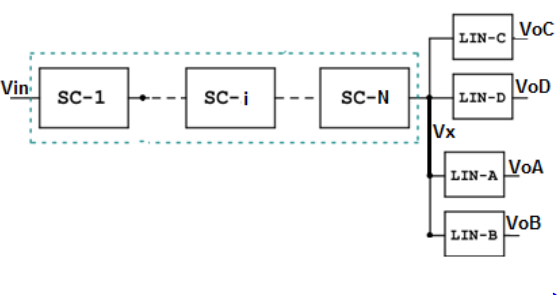
Figure 2. Generic converter architecture based on multi switched capacitor (SC) and linear (LIN) converters
Moreover, each device (e.g., memory, sensor, microcontroller, RF transceiver) in a complex IoT system or CPS may require a different supply voltage level to optimize its performance. Therefore, the power management unit needs more than one output voltage. To this aim, we propose a modular and scalable architecture for the converter (see Figure 2) that can be expanded or reduced in relation to the application.
DESIGNED DC/DC CONVERTER
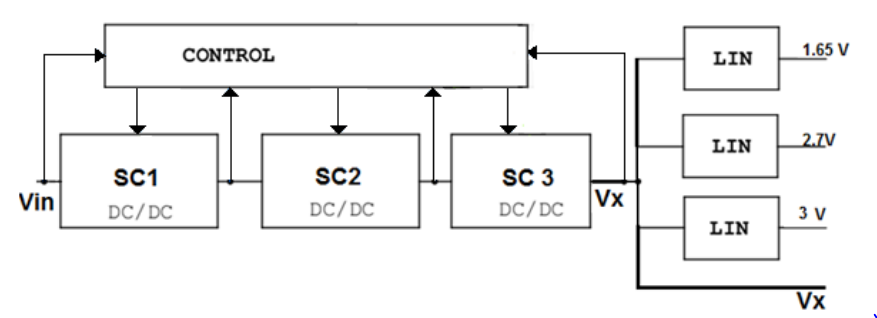
Figure 3. Implemented converter architecture
At the end of the cascade of the three SC converter stages, the global architecture, displayed in Figure 3, has three linear regulators working in parallel to obtain three typical values for the power supply of IoT nodes. Also the Vx value is provided as a fourth output, which is also useful for diagnostic reason.
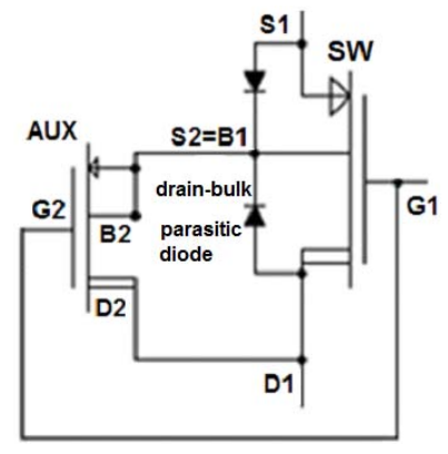
Figure 5. Transistor level design of a switch for high-voltage
The voltage drop on some switches in the circuit, when the converter performs both step-down and step-up conversions, changes from positive to negative and vice versa. In this case a back-to-back circuit switch is needed, which is obtained putting in cascade two structures as in Figure 5, so four transistors are needed. The first stage is in the direction Drain to Source and the following stage is in the opposite direction Source to Drain.
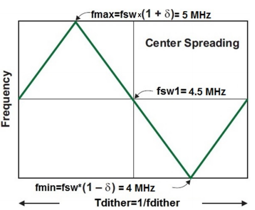
Figure 7. Triangular‐like dithering of the switching frequency
If the switching frequency is constant at a value fSW, then the power spectrum of the system is concentrated at this frequency reaching a very high level, not compliant with regulations for maximum emissions in the environment. The technique of the dithering consists in slightly changing the switching frequency. This allows spreading the power spectrum over a wider range of frequency, thus reducing emission peak value. Once the programmable switching frequency fSW is set, the dithering function periodically changes the switching period according to a triangular law, as in Figure 7.
IMPLEMENTATION RESULTS AND COMPARISON TO THE STATE-OF-THE-ART
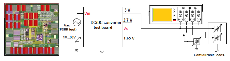
Figure 8. Schematic of the experimental test set-up and chip prototype
The implemented converter has been tested through the experimental laboratory set‐up in Figure 8 where a configurable power supply is used to generate an input DC voltage ranging from 1V to 60V. This variation is needed to measure the line regulation range. In case a PSRR performance measurement has to be done an AC source is placed in series to add a sine wave disturb. The amplitude of the sine wave disturb is Vp = 0.2V if the DC input is in the range 1V to 5V, otherwise Vp is 1V.
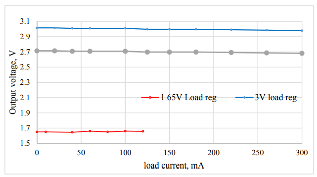
Figure 10. Measured load regulation for the 3V, 2.7V, and 1.65V outputs, when the load current varies from 0 to 300mA for the 3V and 2.7V outputs and from 0 to 120mA for the 1.65V output (Vin = 12V)
Figure 10 shows the load regulation capability of the proposed converter. The output voltage for each of the three outputs is evaluated for different values of the load current in the range from 0 to 300mA for the 3V and the 2.7V outputs and in the range 0 to 120mA for the 1.65V output. In Figure 10, the input voltage is kept at a constant value of 12V.
CONCLUSIONS
A universal and fully-integrated DC/DC converter is proposed in the paper. It aims at minimizing cost and size of power supply systems in wireless nodes for IoT and CPS applications. The proposed converter is made by a cascade of three switching capacitor converters, implementing both step-down and step-up converting ratios, thus regulating all input sources to a voltage of about 4V.
Then, multiple linear regulators are placed at the end of the cascade to provide multiple and stable output voltages to loads such as memories, sensors, processors, wireless transceivers in IoT and CPS nodes. The multi-output power supply regulator has been integrated in a single-chip in a BCD 180nm technology. In this case study, the generation of three output voltages has been considered (3V, 2.7V, and 1.65V, with load current requirements of 0.3A, 0.3A, and 0.12A, respectively).
The proposed converter has the following distinguishing features vs. other state-of-art converters:
(i) It can sustain a wide input voltage range from 1V to 60V. This way it is not optimized for a particular input voltage, but it can be used with changing input power sources, like power harvesting systems and/or very disturbed power supplies;
(ii) It keeps power-efficiency levels up to 70% in the whole input range from 1V to 60V being more efficient than linear regulators and with comparable efficiency to inductor-based regulators;
(iii) The converter avoids the use of inductors and, thanks to the adoption of a high switching frequency up to 5MHz (much higher than the 100kHz adopted by other works in state-of-art converters), the only needed passive components are flying capacitors (whose size is below 10nF) and buffer capacitors (whose size is below 100nF). The total amount of passive devices to be integrated is less than 1µF while in other works, switching around 100kHz: this value is 50 times higher. Hence, the proposed converter can be integrated in a single chip (of 18mm2 for the case study of three output voltages and 2 Watts of total load power), reducing area and assembly effort/cost vs. inductor-based DC/DC converters.
Source: Orcid University
Author: Fernando Gutierrez
>> 50+ IoT based Wireless/GSM Projects for Engineering Students