ABSTRACT
A RF powering circuit used in radio-frequency identification (RFID) tags and other batteryless embedded devices is presented in this paper. The RF powering circuit harvests energy from electromagnetic waves and converts the RF energy to a stable voltage source. Analysis of a NMOS gate-cross connected bridge rectifier is conducted to demonstrate relationship between device sizes and power conversion efficiency (PCE) of the rectifier.
A rectifier with 38.54 % PCE under normal working conditions is designed. Moreover, a stable voltage regulator with a temperature and voltage optimizing strategy including adoption of a combination resistor is developed, which is able to accommodate a large input range of 4 V to 12 V and be immune to temperature variations. Latch-up prevention and noise isolation methods in layout design are also presented.
Designed with the HJTC 0.25 μm process, this regulator achieves 0.04 mV/°C temperature rejection ratio (TRR) and 2.5 mV/V voltage rejection ratio (VRR). The RF powering circuit is also fabricated in the HJTC 0.25 μm process. The area of the RF powering circuit is 0.23 × 0.24 mm2. The RF powering circuit is successfully integrated with ISO/IEC 15693-compatible and ISO/IEC 14443- compatible RFID tag chips.
ARCHITECTURE OF THE RF POWERING CIRCUIT
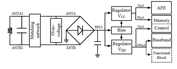
Figure 1. Structure of the RF powering circuit
As shown in Figure 1, the RF powering circuit comp rises four parts. First, the energy harvesting circuit, consisting of an inductor and a resonance capacitor, harvests energy from an electromagnetic field through inductive coupling and resonance. A magnetic coil is used as antenna in this design. Then, the rectifier circuit, which consists of a bridge rectifier and a capacitor, converts the input RF signal from electromagnetic field into a DC signal with ripples.
DESIGN AND IMPLEMENTATION OF RF POWERING CIRCUIT
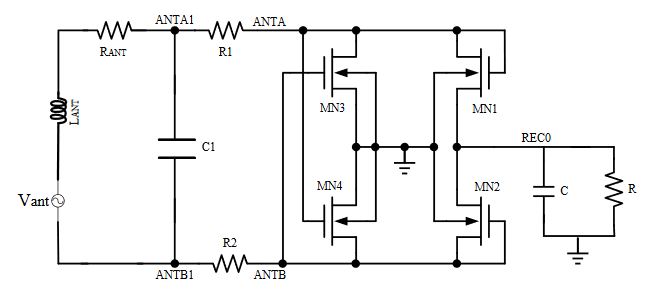
Figure 2. NMOS gate cross-connected bridge rectifier
In Figure 2, the gates of NMOS transistors MN3, MN4 are cross connected to the antennas and MN1, MN2 are connected as diodes. The antenna can be equivalent to an AC voltage source Vant, an inductor LANT and the parasitic resistor RANT. Resistors R1, R2 form the matching circuit, which matches the impedances of the antenna and the rectifier, thus LANT and C1 resonate and the maximum voltage values of ANTA and ANTB will be obtained.
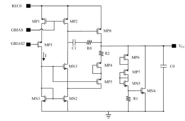
Figure 4. Circuit of VCC regulator
The VCC voltage regulator is shown in Figure 4. By using a combination resistor and a calculation strategy for the device parameters, an optimization for regulator performance related to voltage and temperature is achieved in this work. As can be seen in Figure 4, NMOS transistors MN1 and MN2 form a current mirror.
SIMULATION AND MEASUREMENT RESULTS
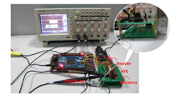
Figure 8. Functional measurement setup based on PCB and the demodulation signal from the tag
The AFE was tested using a TDS 2024B oscilloscope. The test waveform of VCC is shown in Figure 8. The strength of the electromagnetic field surrounding the RFID tag is adjusted by changing the distance between the chip and reader as shown in Figure 8.
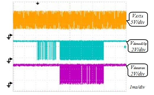
Figure 13. Measured waveform of the communication between reader and tag
The signal Datatran determined by the digital baseband controls the AFE modulator. Figure 13 shows that AFE has realized the information communication with reader successfully, which means this RF powering circuit work normally providing a stable voltage source for the whole chip.
CONCLUSIONS
In this work, a RF Powering circuit used for passive RFID tags is designed and fabricated with the HJTC 0.25 μm CMOS process. The circuit consists of a rectifier, a bias circuit and a regulator. It provides two stable power sources for the analog and digital parts, respectively. The RF powering circuit achieves high PCE of 38.54% with the HJTC 0.25 μm process under normal working conditions and the power supply voltage is immune to temperature and voltage variations.
Simulation results show that this circuit has a TRR = 0.04 mV/°C, and test results show that it has a VRR = 2.5 mV/V. This RF powering circuit is also fabricated with the HJTC 0.25 μm process in the ISO/IEC15693-Compatible and ISO/IEC 14443-Compatible RFID tag chip. Layout of this chip is optimized for latch-up prevention and noise isolation. Measurement results of the tag show that this circuit can provide a stable voltage source for a HF RFID tag chip for its proper operation.
Source: Huazhong University
Authors: Dong sheng Liu | Rencai Wang | Ke Yao | Xue cheng Zou | Liang Guo
>> 60+ Final Year Projects on Microstrip Antenna Design for Engineering Students