ABSTRACT
Digital Radio Frequency Memories (DRFM) are widely used as modules in digital signal processing. These modules can provide several forms of signal manipulation and storage capabilities. With single event effects caused by environmental radiation the need for a radiation hardened DRFM is increased. Typical radiation hardening involves the use of specialized foundries utilizing proprietary CMOS libraries that are expensive to build or adding lead packages around a chip that is expensive and add weight to the chip. An alternative radiation hardening technique is to utilize a radiation hardened by design library.
This library includes digital gates that have been hardened by the use of guard rings, reverse body bias or other methods. With the use of the hardened library, commercial synthesis tools can create a structural Verilog output from the behavioral VHDL design. The radiation hardened by design circuit will be larger than a non-hardened design, but can be fabricated using standard foundries. This research also takes advantage of current advancements of commercially available software and designs that have led to a structured ASIC approach for fabricating a design.
This structured ASIC approach fabricates a design in two stages. The first stage is the transistor and bottom metal layers with the second stage being the top metal layers. Silicon wafers can be fabricated in bulk using the first stage of uncommitted logic with separate top metal layer masks applied to commit the logic to a specific design. A radiation hardened by design standard cell library was used to create the Structured ASIC standard cells and will allow production of radiation hardened circuits with a short design time.
For this research, a generic frequency shifting DSSM is proposed that targets a radiation hardened by design Structured ASIC to deliver performance in processing as well as radiation hardening at both the transistor level and gate level. This re-search produces a parameterizable DSSM VHDL design that can be easily modified to produce a DSSM with various signal processing and storage capabilities with minimal modifications. The designed DSSM was tested on an FPGA board for prototyping, but was ultimately targeted for the radiation hardened by design structured ASIC. The design created through this research was compared to a non-hardened DSSM using a similar CMOS process for area, power, speed and Spur Free Dynamic Range.
BACKGROUND AND THEORY
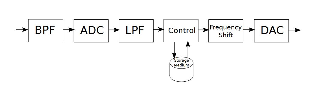
Figure 2.1: High-Level Overview of DRFM
A possible high-level view of a DRFM for the EW environment is shown in Figure 2.1. This figure shows the optional Bandpass Filter (BPF), which can be used to select different bands of interest in the RF spectrum. Also included is the Low-pass Filter (LPF) used to increase the single to noise ratio.
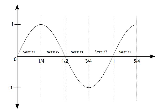
Figure 2.7: Symmetry Exploitation of Quarter-Wave Technique
The simplest approach to create a DDS uses a quarter-wave approximation technique where one-quarter of a full period is loaded into memory elements and the desired output signal frequency is obtained by the repeat ed addressing of the memory elements. Figure 2.7 shows the symmetry that is exploited in this DDS method. If the memory elements are read in sequential order to produce region 1, then reading the elements in reverse order will produce region 2.
METHODOLOGY
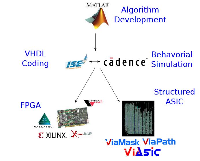
Figure 3.4: Design Flow
The flow of the DSSM design in this research was targeted at creating a semi-generic VHDL design file that can be synthesized to an S-ASIC, but many other steps needed to be taken first. As shown in Figure 3.4, the design flow began with a model of the algorithm, then moved into the VHDL design and simulated using both the Cadence Sim Vision simulation suite and an FPGA. After successful simulations, the design could be synthesized, placed, routed and then re-simulated to verify correctness before fabricating the design.
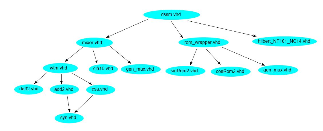
Figure 3.12: VHDL File Dependency
If the bit width of the ROM samples is modified, the NC and NCO generic parameters must be checked. It is possible for a generating application to be created in which the given parameters for both the Hilbert filter and the ROM are provided by the user and VHDL entities are generated for shorter modification times and easy implementation. Figure 3.12 shows the dependency tree for the VHDL design files needed to simulate and synthesize the DSSM design.
ANALYSIS AND RESULTS
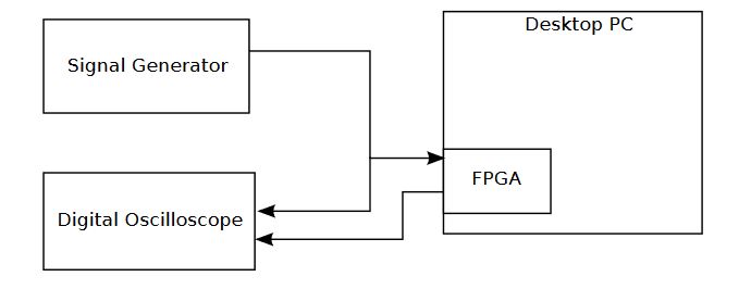
Figure 4.1: FPGA Test Setup
The setup for the FGPA testing was created using the block diagram shown in Figure 4.1, with one signal generator providing the single-tone input. This output is then connected through a splitter to both the FPGA ADC input and the digital oscilloscope. The digital oscilloscope us ed included a Fast Fourier Transform (FFT) function that would allow the oscilloscope to show the spectral content. The output of the DSSM was connected to the second channel on the oscilloscope for comparison with the input signal.
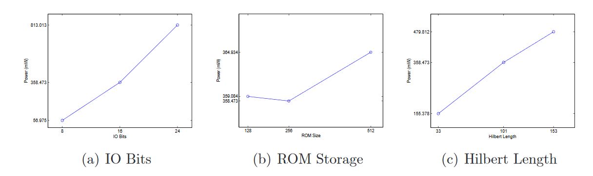
Figure 4.25: Design Parameters vs. Power Comparison
The first to look at is the power for the S-ASIC design and was calculated from the Cadence RTL Compiler output files. As can be seen from the the plots in Figure 4.25, both the length of the Hilbert filter as well as the IO bit width greatly influenced the power needed for the DSSM.
CONCLUSIONS
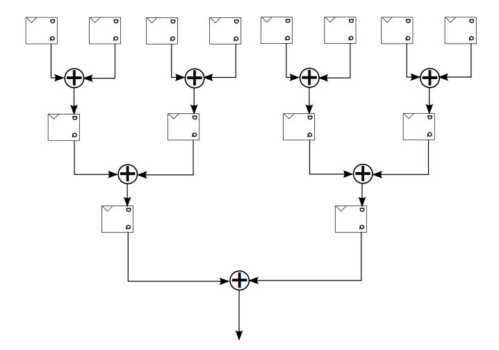
Figure 5.2: Pipelined Adder Tree for Hilbert Filter
The same basic filter structure can be utilized with the addition of DFFs between the adders in the adder tree. If a new design includes more DFFs, then the entire tree may be pipelined as shown in Figure 5.2. If the number of DFFs is limited, as it was in this DSSM design, there should be several iterations completed to insert the needed pipeline stages in strategic locations such that the speed of the DSSM can be increased without the over utilization of the available DFFs.
Source: Wright State University
Author: Thomas B. Pemberton